Structural and Optical Properties of Multilayered Cobalt/M (with M= Platinum or Rhodium) Thin Films Nanowires Electrodeposited into Ion Track-Etched Polycarbonate Membra
*Corresponding Author(s):
A Kazadi Mukenga BantuDepartment Of Physics Materials And Nanoscience Group, University Of Kinshasa, Kinshasa, Congo, The Democratic Republic Of The
Tel:+24 3811441644; +24 3819206439,
Email:albert.kazadi@unikin.ac.cd; fakazadi@gmail.com
Abstract
A series of multilayered cobalt/M (M= platinum, rhodium) thin films nanowires with diameter Dp=400 nm were synthesized into ion track-etched polycarbonate membranes by electrodeposition. Scanning Electron Microscopy (SEM) displays cylindrical wires with smooth and homogeneous contours. X-Ray Diffraction (XRD) results revealed that all samples had a mixture of Hexagonal Close-Packed (HCP) and Face Centered Cubic (FCC) phases. The wires exhibit magnetic anisotropy, which is observed and is ascribed to shape anisotropy. The magnetization reversal strongly depends on the variation of the thickness between cobalt and M (M=Pt, Rh) layers. Absolute reflectance spectra of multilayered cobalt/M (M=platinum, rhodium) thin films nanowires were acquired over the range 800-2500 nm using a Cary 5000 UV-Visible-Near Infra Red Spectrophotometer. The optical specular reflectance spectrum shows a band which probably originates from a surface plasmon resonance. Therefore, the change of the thickness (wires length) was seen to control the properties of the multilayered thin films nanowires and hence their properties could be modified for desired purpose.
PACS: 75.70.-i Magnetic thin films and multilayers - 81.15.Pq Electrodeposition, Reflectance, nanowires.
INTRODUCTION
MATERIALS AND METHODS
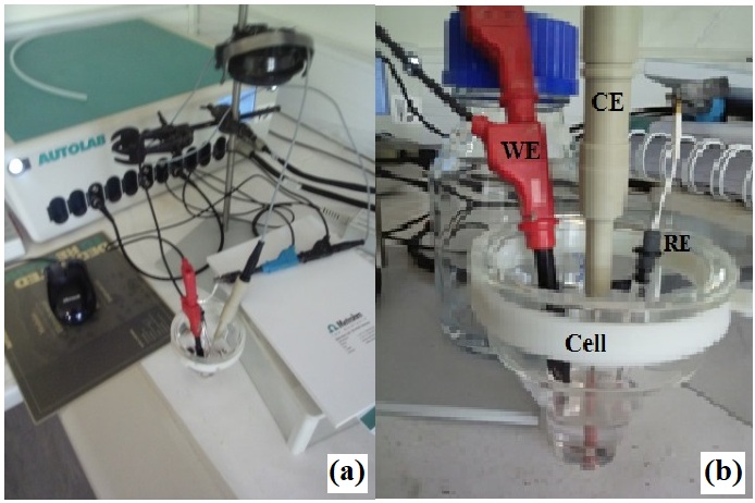
Figure 1: (a) Autolab PGSTAT, and (b) Electrochemical Cell with the three electrodes
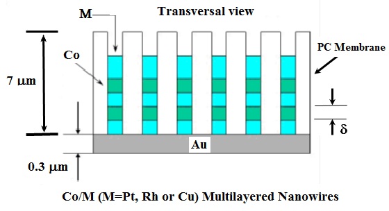
Polycarbonate (PC) membranes (from Millipore) of thickness δ≈7 mm and pores diameter ranging from 100 to 400 nm were used to produce multilayered Co/M (M=Pt, Rh) thin films nanowires. A gold (Au) seed layer was first evaporated on the backside of the PC porous membrane to cover the pores. And this backing layer served as cathode (working electrode WE) during the subsequent electrochemical deposition of the multilayered Co/M thin films nanowires. During the deposition, a negative constant voltage was applied for Co and M reduction respectively and the electric current was monitored as a function of time. The multilayered Co/M thin films nanowires were prepared alternating elemental target into PC template. The substrates dimension was (25px7x10-3) mm3. The figure 2 shows the schematic transversal view of the PC membrane where d is the thickness of the alternating deposited element Co or M.
The electrolyte used in this work consisted of an aqueous solution as shown in the following table N° 1. To avoid the element M in the cobalt layer during the electrodeposition, we took the concentration of cobalt 100 times the concentration of the element M.
|
Product name |
Concentration [mM] |
|
|
CoSO4·7H2O (99,9%) |
1 |
100 |
|
M=K2PtCl6 or RhCl3 (99,8 %) |
0.01 |
1 |
|
H3BO4 (99,5 %) |
40 |
|
The morphology of the thin films wires were studied by means of Scanning Electron Microscopy (SEM). For this last purpose, the PC membrane template was dissolved in ones drops of dichloromethane (CH2Cl2).
In addition, the microstructure and optical properties of the wire arrays were investigated by X-Ray Diffraction (XRD), the optical reflectance of the as-prepared multilayered Co/M thin films nanowires has been characterized using UV-Visible-Near Infrared Spectrophotometer (Agilent Technologies Cary Series 5000 UV-Vis-NIR Spectrophotometer) equipped with an integrating device. Reflectance spectra of the samples were measured at Room Temperature (RT) between 800nm and 2500nm. All measurements were performed in double beam mode, using reduced slit height and zero/baseline correction. Prior to the measurements, each sample was positioned using the sample clip while baseline correction was performed before the acquisition of sample spectra in order to set 0 and 100% Transmission (T) values. This is particularly important when measuring samples with low reflectance.
RESULTS AND DISCUSSION
Electrodeposition processus
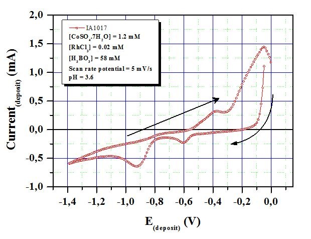
The curve show the cathodic and anodic peaks associated to the deposition and dissolution of cobalt, respectively. There is no considerable current flowing in the potential region between 0.0 V and -1.4 V. Cobalt depositions begin at around -0.9 V. As the absolute value of cathode potential increases from -0.80 V to -1.2 V, the current also increases. Between -1.2 V and -1.4 V, the increase of current slows down. After -1.4 V, it begins to increase with the increase of the potential. When the scan is reversed, the nucleation loop is observed. At around -0.05 V an oxidation peak of cobalt is detected. According to these results and the appearance of the films, the optimum electrodeposition potential range was decided to be from -0.80 V to -1.20V. The selected potential value is Ed (Co)≈-0.90V. The same was done for M deposition potential which was decided to be Ed (M)≈- 0.65V. Multilayered Co/M thin films NWs were synthesized alternatingly switching cathode potential from -0.65 V (for M layer) to -0.90 V (for Co layer) as shown in figure 4. The current-time transients were also recorded to understand the nucleation and growth mechanism of Co/M thin films nanowires. Figure 4 shows the (a) potential-time curve and (b), (c) and (d) current-time transients of the thin films nanowires.
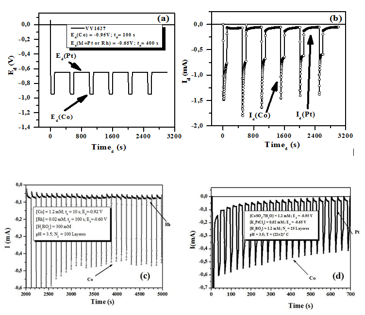
According to this figure, when the potential is switched from -0.90 V to -0.65 V, anodic current is observed for Co/Pt. This is resulting from the dissolution of electrodeposited Co, because -0.65V is nobler than the equilibrium potential of Co. At this potential, it is estimated that the Pt deposition and Co dissolution will proceed simultaneously. According to the time - dependence of cathodic current during electrodeposition of Co/Pt multilayered nanowires as shown in figure 4(d), filling time was around 10000 s and the deposition rate was estimated to be about ≈0.7 nm/s.
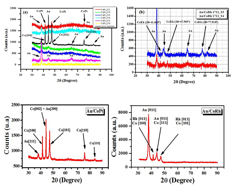
XRD characterization
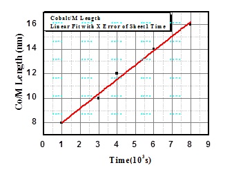
In figure 6, we could observe that the wires thickness has linear relationship with respect to the synthesis time. This indicates that there is indeed a linear relationship between the length of the nanowires and the above-mentioned time for each deposition potential.
SEM and AFM characterization
|
Parameter |
Value |
|
Pore diameter [nm] |
≈ 400 |
|
Membrane thickness [μm] |
≈ 7 |
|
Pore density [pores/cm2] |
≈ 2x10⁶ |
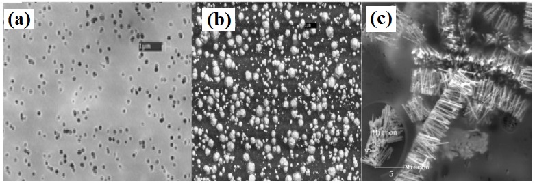
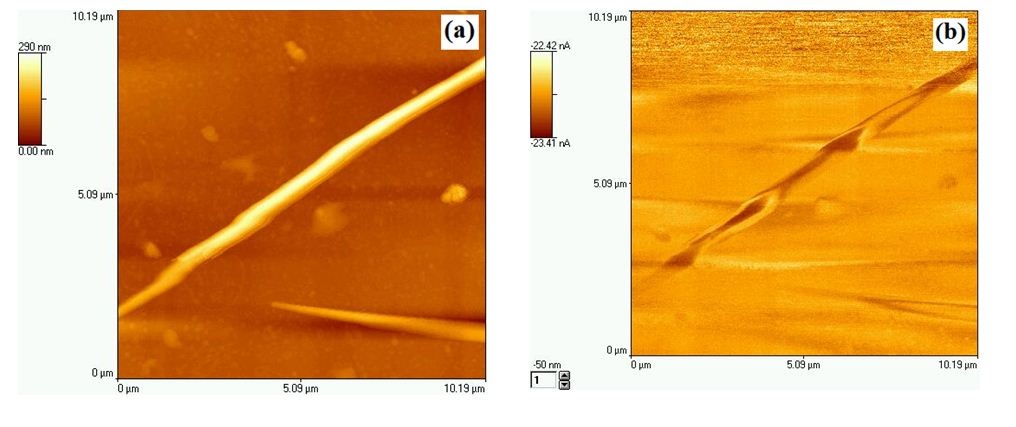
The SEM micrograph shown in figure 7(a) displays the morphology and size of PC template before deposition of the Co/M nanowires. And the figure 7(b) shows the top surface of PC template with hemispherical caps formed after deposition. The wires are aggregated and randomly distributed on the substrate. The wire aggregation is ascribed to surface tension effects of solvent droplets when drying the sample after template dissolution. The detailed description of this phenomenon can be found elsewhere [22]. The SEM image presented in figure 9 and the AFM image in figure 8(a) reveal that the wires have excellent cylindrical smooth shape (highly polished surfaces), uniform deposit and homogeneous contours along their long axis. From figure 8(b), the MFM image shows the magnetic configuration of as-grown thin films, observed by magnetic force microscopy. One could notes that the magnetization is perpendicular to the wires axis in conformity to the result found for the Co wires. The polarity alternation suggests the reversal of magnetization in the perpendicular plane in function of wires’ length.
Optical characterization
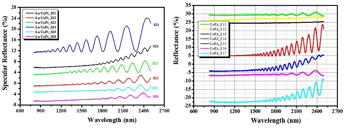
Figure 9: Total reflection spectra of our two series (CoPt and CoRh) of samples as electrodeposited.
As far as we know, this reflectance oscillation could be also due to the oscillatory exchange coupling across the nonmagnetic layers M in Cobalt layers as function of thickness of M layers. It follows that the oscillations in these systems are approximately periodic, and the period change with the change of thickness. This phenomena has been discovered by Parkin et al., [1]. Therefore, it is expected that the cylindrical shape of the nanowires has a significant influence on their optical properties.
CONCLUSION
ACKNOWLEDGEMENT
One of the authors (Prof. Dr A. Kazadi Mukenga Bantu) would like to express his appreciation and thanks to Prof. M. Maaza Nanosciences African network (NANOAFNET), Materials Research Department (MRD), iThemba LABS-National Research Foundation (NRF), Somerset West, South Africa for his valuable suggestions, fruitful discussion, availability, constant support, help and encouragement. Also very heartfelt thanks to all the staff members of the Materials Research Group (MRG-iThemba Labs) for giving me the opportunity, time and facilities to complete this work.
REFERENCES
- Parkin SS, More N, Roche KP (1990) Oscillations in exchange coupling and magnetoresistance in metallic superlattice structures: Co/Ru, Co/Cr, and Fe/Cr. Phys Rev Lett 64: 2304-2307.
- Bruno P, Chappert C (1991) Oscillatory coupling between ferromagnetic layers separated by a nonmagnetic metal spacer. Phys Rev Lett 67: 1602-1605.
- Fert AR (1991) Magnetic and Transport Properties of Metallic Multilayers. Materials Science Forum 59: 439-480.
- Kuchibhatla SVNT, Karakoti AS, Bera D, Seal S (2007) One dimensional nanostructured materials. Prog Mater Sci 52: 699-913.
- Ross CA (2001) Patterned Magnetic Recording Media. Annu Rev Mater Res 31: 203-235.
- Vila L, Vincent P, Pra LDD, Pirio G, Minoux E, et al. (2004) Growth and Field-Emission Properties of Vertically Aligned Cobalt Nanowire Arrays. Nano Lett 4: 521-524.
- Xavier S, Mátéfi-Tempfli S, Ferain E, Purcell S, Enouz-Védrenne S, et al. (2008) Stable field emission from arrays of vertically aligned free-standing metallic nanowires. Nanotechnology 19:
- Huang X, Li L, Luo X, Zhu X, Li G (2008) Orientation-Controlled Synthesis and Ferromagnetism of Single Crystalline Co Nanowire Arrays. J Phys Chem C 112: 1468-1472.
- Niu H, Chen Q, Zhu H, Lin Y, Zhang X (2003) Magnetic field-induced growth and self-assembly of cobalt nanocrystallites . J Mater Chem 13: 1803-1805.
- Thurn-Albrecht T, Schotter J, Kästle GA, Emley N, Shibauchi T, et al. (2000) Ultrahigh-density nanowire arrays grown in self-assembled diblock copolymer templates. Science 290: 2126-2129.
- Liu J, Duan JL, Toimil-Molares ME, Karim S, Cornelius TW, et al. (2006) Electrochemical fabrication of single-crystalline and polycrystalline Au nanowires: the influence of deposition parameters. Nanotechnology 17:
- Whitney TM, Jiang JS, Searson PC, Chien CL (1993) Fabrication and Magnetic Properties of Arrays of Metallic Nanowires. Science 261: 1316-1319.
- Piraux L, George JM, Despres JF, Leroy C, Ferain E, et al. (1994) Giant magnetoresistance in magnetic multilayered nanowires. Appl Phys Lett 65: 484-486.
- Blondel A, Meier JP, Doudin B, Ansermet JP (1994) Giant magnetoresistance of nanowires of multilayers. Appl Phys Lett 65: 3019-3021.
- Cornelius TW, Brötz J, Chtanko N, Dobrev D, Miehe G, et al. (2005) Controlled fabrication of poly- and single-crystalline bismuth nanowires. Nanotechnology 16:
- Bantu AKM, Rivas J, Zaragoza G, López-Quintela MA, Blanco MC (2001) Structure and magnetic properties of electrodeposited cobalt nanowires. J Appl Phys 89: 3393-3397.
- Maurer F, Brötz J, Karim S, Toimil Molares ME, Trautmann C, et al. (2007) Preferred growth orientation of metallic fcc nanowires under direct and alternating electrodeposition conditions. Nanotechnology 18:
- Ni X, Ma J, Li J, Huang J, Jiao D, et al. (2008) Structure and microwave characteristics of Co/TiO2 nanocomposites prepared by ball milling. J Nanosci Nanotechnol 8: 4470-4476.
- Huang JY, Wu YK, Ye HQ (1996) Deformation structures in ball milled copper. Acta Mater 44: 1211-1221.
- Nakahara S, Mahajan S (1980) The Influence of Solution pH on Microstructure of Electrodeposited Cobalt. J Electrochem Soc 127: 283-288.
- Bantu AKM, Castro ACDE, Magalhaes SDDE, Barthem VMTS, Givord D, et al. (2014) Structural and Magnetic Properties of Electrodeposited CoPt and FeCu Nanowires Embedded in Polycarbonate Membranes. The African Review of Physics 9: 487-496.
- Duan J, Liu J, Yao H, Mo D, Hou M, et al. (2008) Sci Eng 57.
- Kreibig U, Vollmer M (1995) Optical Properties of Metal Clusters. Springer 25: 532.
Citation: Bantu AKM, Saleh K, Maaza M(2019) Structural and Optical Properties of Multilayered Cobalt/M (with M= Platinum or Rhodium) Thin Films Nanowires Electrodeposited into Ion Track-Etched Polycarbonate Membranes. J Nanotechnol Nanomed Nanobiotechnol 6: 024.
Copyright: © 2019 A Kazadi Mukenga Bantu, et al. This is an open-access article distributed under the terms of the Creative Commons Attribution License, which permits unrestricted use, distribution, and reproduction in any medium, provided the original author and source are credited.